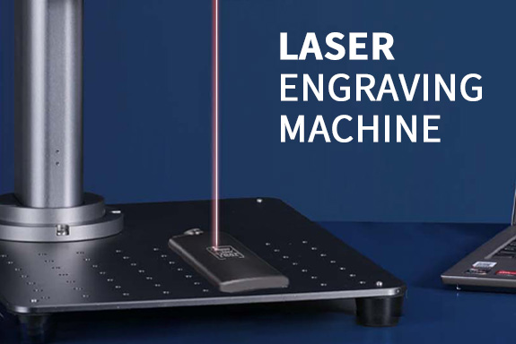
In the world of electronic manufacturing, precision is key, especially when it comes to resistors and circuit components. Laser trimming equipment is a groundbreaking technology that allows manufacturers to achieve exceptional accuracy in adjusting the resistance of components like thin resistors and even delicate laser wafer trimming. This article will explore how laser circuit trimming works, the role of thin resistors in advanced circuits, and how laser trimming equipment is revolutionizing the precision manufacturing of resistors and wafers.
What is Laser Trimming Equipment?
Laser trimming equipment refers to specialized machines that use focused laser beams to precisely alter the resistance value of a resistor or adjust circuit elements in a printed circuit board (PCB). The process works by selectively removing material from a resistor or circuit trace with high precision, enabling the fine-tuning of electrical characteristics.
Laser trimming is particularly useful when traditional mechanical trimming techniques fall short, offering a much more accurate and non-invasive method for trimming resistors, capacitors, and even entire circuits on a wafer.
Laser Circuit Trim: Enhancing Precision in Electronics
Laser circuit trimming is the process of using a laser to adjust the resistance of various components on a printed circuit board (PCB) or even entire circuit elements within a semiconductor. This process can target specific areas on a circuit, allowing for precise calibration of resistance values and ensuring that the circuit operates within the desired specifications.
Key Benefits of Laser Circuit Trimming:
- Increased Accuracy: The precision of laser cutting ensures that adjustments are made down to the micron level, which is crucial for high-performance electronics such as medical devices and telecommunications equipment.
- Non-Contact Process: Unlike mechanical trimming, laser trimming is non-contact, which prevents physical damage to the circuit and maintains the integrity of delicate components.
- Customization: Laser circuit trimming allows for tailored resistance values, providing flexibility for custom circuit designs and performance requirements.
This technique is often used in high-frequency circuits, sensors, and calibration applications, where exact resistance values are critical.
The Role of Thin Resistors in Laser Trimming
Thin resistors are resistive elements that are constructed using thin films of resistive material, often deposited onto a substrate. These resistors are commonly used in applications where precise resistance values and compact size are needed. Laser trimming is ideal for fine-tuning thin resistors, allowing manufacturers to achieve the exact resistance required for specific electronic applications.

Advantages of Thin Resistors:
- Compact Size: Thin resistors are typically smaller than traditional thick-film resistors, making them ideal for high-density, miniaturized circuit boards.
- High Precision: Thin-film resistors can be manufactured to extremely tight tolerances, and laser trimming enhances this precision by offering a fine degree of adjustment without the risk of over-trimming.
- Cost-Effective: While initial manufacturing costs might be higher, thin resistors offer better performance and longevity, making them more cost-effective in the long run.
Laser trimming helps achieve the high precision needed for thin resistors, which are commonly found in advanced consumer electronics, telecommunications, and automotive applications.
Laser Wafer Trimming: Fine-Tuning Semiconductor Components
Laser wafer trimming is an advanced technique used to modify the resistance and electrical characteristics of semiconductor wafers during the manufacturing process. This technique is especially useful for adjusting resistance values in thin-film resistors and fine-tuning integrated circuits (ICs) on the wafer itself.
Key Features of Laser Wafer Trimming:
- Precision at the Micron Level: Laser trimming can precisely remove material from specific locations on the wafer, allowing for micro-level adjustments to components like resistors, capacitors, and even the wafer itself.
- Non-Destructive: Since it is a non-contact process, laser wafer trimming preserves the integrity of the wafer and its components, making it ideal for fine-tuning sensitive semiconductor devices.
- Cost-Effective for High-Volume Production: The ability to perform trimming directly on the wafer eliminates the need for additional steps or processes, improving overall production efficiency.
Laser wafer trimming is commonly used in the production of microelectronics, semiconductors, and MEMS devices, where accuracy is critical and component adjustments must be made at the wafer level.
Conclusion: The Future of Laser Trimming Equipment
As the demand for higher precision in electronics continues to grow, laser trimming equipment is poised to become an essential part of the manufacturing process. Whether it’s for laser circuit trimming, adjusting thin resistors, or laser wafer trimming, the ability to make precise, non-contact adjustments is invaluable in ensuring that components meet the exact specifications required for optimal performance.
With its ability to deliver high precision, increase production efficiency, and reduce material waste, laser trimming technology is becoming increasingly important in industries ranging from consumer electronics to semiconductors and medical devices.
By incorporating laser trimming into the production process, manufacturers can achieve unprecedented levels of accuracy, improving the performance and reliability of their products while maintaining cost-effectiveness. Whether working with thin resistors, laser circuit trims, or laser wafer trimming, this advanced technology will continue to shape the future of precision electronics manufacturing.
由用户投稿整理稿件发布,不代表本站观点及观点,进行交流学习之用,如涉及版权等问题,请随时联系我们(yangmei@bjjcz.com),我们将在第一时间给予处理。


